/* Put rfMaxima.mac in the same directory as this notebook, or add its
   directory to file_search_maxima. */
load("rfMaxima.mac")$RF CMOS SPST Switch
Generated from RF_CMOS.wxm with rfMaxima 0.2.5 on Maxima 5.46.0.
All results were computed by executing the notebook; none is transcribed.
https://qucs.sourceforge.net/docs/report/EKV26.pdf
https://ngspice.sourceforge.io/external-documents/models/ekv_v262.pdf
(parameter set formerly published by EPFL at legwww.epfl.ch/ekv/paramset.html; no longer online)
EKV v2.6 Parameters for 0.5 um CMOS (EPFL-LEG, 1999)
ELDO (LEVEL = 44) / PSPICE (LEVEL = 5) example parameter set for the EKV v2.6 model is provided for NMOS and PMOS.
IMPORTANT NOTES: ---------------- Parameters do not correspond to a particular technology but have reasonable values for standard 0.5um CMOS. Not intended for use in real design.
Includes all intrinsic model parameters. An example set for extrinsic model parameters is provided.
Geometry range: W >= 0.8um, L >= 0.5um
Voltage range: |Vgb| < 3.3V, |Vdb| < 3.3V, |Vsb| < 2V
For use with either simulator, comment/uncomment respective lines. Use of extrinsic model parameters and models (series resistance, junction currents/capacitances) is in general simulator-dependent.
Description [Unit], SPICE Symbol Channel length [m], L Channel width [m], W Parallel multiple device number [], NP Series multiple device number [], NS Gate oxide capacitance per unit area [F/m^2], COX Junction length [m], XJ Channel width correction [m], DW Channel length correction [m], DL Long-channel threshold voltage [V], VTO Body effect parameter [sqrt(V)], GAMMA Bulk Fermi potential [V], PHI Transconductance parameter [A/V^2], KP Mobility reduction coefficient [1/V], THETA Threshold voltage temperature coefficient [V/K], TCV Heavily doped diffusion length [m], HDIF Drain-source diffusion sheet resistance [Ohm/sq.], RSH Source contact resistance [Ohm], RSC Drain contact resistance [Ohm], RDC Gate to source overlay capacitance[F/m], CGSO Gate to drain overlay capacitance [F/m], CGDO Gate to bulk overlay capacitance [F/m], CGBO Diode emission coefficient [], N Leakage current [A], IS Reverse breakdown voltage [V], BV Current at Bv [A], IBV Junction potenVial [V], VJ Zero bias depletion capacitance [F], CJ Grading coefficient [], M Relative area [], AREA Forward-bias depletion capcitance coefficient [], FC Transit time [s], TT Saturation current temperature exponent [], XTI Flicker noise coefficient [], KF Flicker noise exponent [], AF Parameter measurement temperature [deg. Celsius], TNOM Device temperature [deg. C], TEMP
NMOS
Process Related Model Parameters
COX:3.45E-3$
XJ:0.15E-6$
Intrinsic Model Parameters
VTO:0.6$
GAMMA:0.71$
PHI:0.97$
KP:150E-6$
E0:88.0E6$
UCRIT:4.5E6$
DL:-0.05E-6$
DW:-0.02E-6$
LAMBDA:0.23$
LETA:0.28$
WETA:0.05$
Q0:280E-6$
LK:0.5E-6$
Substrate Current Parameters
IBN:1.0$
IBA:200E6$
IBB:350E6$
Intrinsic Model Temperature Parameters
TNOM:25.0$
TCV:1.5E-3$
BEX:-1.5$
UCEX:1.7$
IBBT:0.0$
1/f Noise Model Parameters
KF:1E-27$
AF:1$
Series Resistance and Area Calulation Parameters
HDIF:0.9E-6$
RSH:510$
Junction Current Parameters
JS:8.0E-6$
JSW:1.5E-10$
XTI:0$
N:1.5$
Junction Capacitances Parameters
CJ:8.0E-4$
CJSW:3.0E-10$
MJ:0.5$
MJSW:0.3$
PB:0.9$
PBSW:0.5$
FC:0.5$
Gate Overlap Capacitances
CGSO:1.5E-10$
CGDO:1.5E-10$
CGBO:4.0E-10$
PMOS
Process Related Model Parameters
COX:3.45E-3$
XJ:0.15E-6$
*** Intrinsic Model Parameters
VTO:-0.55$
GAMMA:0.69$
PHI:0.87$
KP:35.0E-6$
E0:51.0E6$
UCRIT:18.0E6$
DL:-0.05E-6$
DW:-0.03E-6$
LAMBDA:1.1$
LETA:0.45$
WETA:0.0$
Q0:200E-6$
LK:0.6E-6$
Substrate Current Parameters
IBN:1.0$
IBA:0.0$
IBB:300E6$
Intrinsic Model Temperature Parameters
TNOM:25.0$
TCV:-1.4E-3$
BEX:-1.4$
UCEX:2.0$
IBBT:0.0$
1/f Noise Model Parameters
KF:1.0E-28$
AF:1$
Series Resistance and Area Calulation Parameters
HDIF:0.9E-6$
RSH:990$
Junction Current Parameters
JS:4.0E-5$
JSW:7.0E-10$
XTI:0$
N:1.8$
Junction Capacitances Parameters
CJ:8.0E-4$
CJSW:4.0E-10$
MJ:0.5$
MJSW:0.35$
PB:0.9$
PBSW:0.8$
FC:0.5$
Gate Overlap Capacitances
CGSO:1.5E-10$
CGDO:1.5E-10$
CGBO:4.0E-10$
Device Under Analysis (NMOS)
IMPORTANT: the NMOS and PMOS blocks above use the SAME symbol names, so the PMOS cell overwrites every NMOS value. rfMaxima 0.2.4 then evaluated the "NMOS" switch below with PMOS parameters (VTO = -0.55 V, KP = 35 uA/V^2, RSH = 990 Ohm/sq). Re-assert the NMOS set here, explicitly, immediately before the device analysis.
COX:3.45E-3$ XJ:0.15E-6$
VTO:0.6$ GAMMA:0.71$ PHI:0.97$ KP:150E-6$
E0:88.0E6$ UCRIT:4.5E6$ DL:-0.05E-6$ DW:-0.02E-6$
LAMBDA:0.23$ LETA:0.28$ WETA:0.05$ Q0:280E-6$ LK:0.5E-6$
HDIF:0.9E-6$ RSH:510$
CJ:8.0E-4$ CJSW:3.0E-10$ MJ:0.5$ MJSW:0.3$ PB:0.9$ PBSW:0.5$ FC:0.5$
CGSO:1.5E-10$ CGDO:1.5E-10$ CGBO:4.0E-10$
KF:1E-27$ AF:1$
Small Signal RF Model
%epsilon_Si:104.5e-12$
%epsilon_ox:34.5e-12$
q:1.602e-19$
k:1.3807e-23$
TOX:34.5e-12/COX;
UO:KP/(COX)*10000;
LD:CGDO/COX;/* The EKV set above is documented as valid for W >= 0.8 um and L >= 0.5 um
("reasonable values for standard 0.5um CMOS ... Not intended for use in
real design"). 0.2.4 evaluated it at L = 0.13 um, four times outside that
range. For a 130 nm switch, load a 130 nm parameter set instead. */
L:0.5e-6$
W:10e-6$Assuming strong inversion, linear region
ON State (VGS>VTO, VDS=0V)
COX gives rise to three capacitances:
- an overlap capacitance between gate and source: CGSO*W
- a gate to channel capacitance, equally divided between source and drain: COX*W*L/2
- an overlap capacitance between gate and drain: CGDO*W
VGS:3;
CGS:COX*W*L/2+CGSO*W;
CGD:COX*W*L/2+CGDO*W;
CSB:CJ*W*HDIF+CJSW*2*(W+HDIF);
CDB:CJ*W*HDIF+CJSW*2*(W+HDIF);
RDS:1/(KP*W/L*(VGS-VTO));
ZDS:(1/RDS+(1/(s*CGS)+1/(s*CGD))^(-1))^(-1);
S_SIMPLE:ABCD2S(ABCD_SeriesImpedance(ZDS));
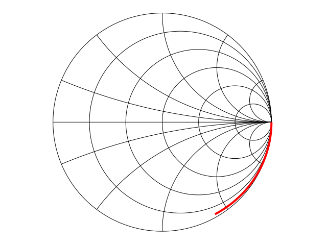
S:ABCD2S(ABCD_ShuntAdmittance(s*CSB).ABCD_SeriesImpedance(ZDS).ABCD_ShuntAdmittance(s*CDB));define(S11(s),block([Z_0],Z_0:50,ev(S[1,1])))$
S11(s);
PlotSmithChart([
parametric,
realpart(S11(%i*%omega)),
imagpart(S11(%i*%omega)),
[%omega,2*%pi*1e6,2*%pi*100e9],
[nticks,1000]]);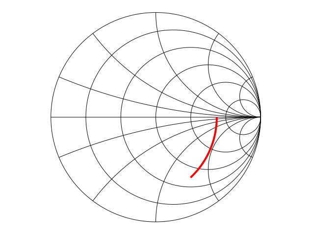
define(S12(s),block([Z_0],Z_0:50,ev(S[1,2])))$
S12(s);
/* S12 is a TRANSMISSION coefficient; a Smith chart maps REFLECTION
   coefficient.  Plot its magnitude against frequency instead. */
wxplot2d(20*log10(cabs(S12(%i*2*%pi*f*1e9))),
    [f,0.001,100],
    [logx],
    [legend,false],
    [xlabel,"Frequency [GHz]"],
    [ylabel,"dB20(|S12|) [dB]"],
    [style,[lines,3,2]],
    [gnuplot_preamble,"set grid"]);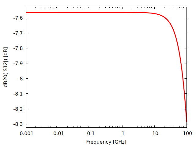
define(S21(s),block([Z_0],Z_0:50,ev(S[2,1])))$
S21(s);
/* S21 is a TRANSMISSION coefficient; a Smith chart maps REFLECTION
   coefficient.  Plot its magnitude against frequency instead. */
wxplot2d(20*log10(cabs(S21(%i*2*%pi*f*1e9))),
    [f,0.001,100],
    [logx],
    [legend,false],
    [xlabel,"Frequency [GHz]"],
    [ylabel,"dB20(|S21|) [dB]"],
    [style,[lines,3,2]],
    [gnuplot_preamble,"set grid"]);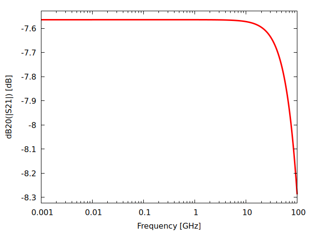
define(S22(s),block([Z_0],Z_0:50,ev(S[2,2])))$
S22(s);
PlotSmithChart([
    parametric,
    realpart(S22(%i*%omega)),
    imagpart(S22(%i*%omega)),
    [%omega,2*%pi*1e6,2*%pi*100e9],
    [nticks,1000]]);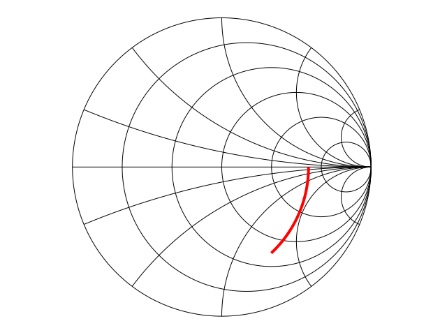
OFF State (VGS=0V, VDS=0V)
VGS:0;
CGS:COX*W*L/2+CGSO*W;
CGD:COX*W*L/2+CGDO*W;
CSB:CJ*W*HDIF+CJSW*2*(W+HDIF);
CDB:CJ*W*HDIF+CJSW*2*(W+HDIF);
/* 0.2.4 had RDS:RSH*W/L here.  RSH counts SQUARES, so the number of squares
   is L/W, not W/L -- and in any case an OFF channel is not an RSH-defined
   resistor: the isolation is set by C_off (below) with subthreshold leakage
   on top.  The line was also never used: ZDS below is purely capacitive. */
ZDS:1/(s*CGS)+1/(s*CGD);
S_SIMPLE:ABCD2S(ABCD_SeriesImpedance(ZDS));
S:ABCD2S(ABCD_ShuntAdmittance(s*CSB).ABCD_SeriesImpedance(ZDS).ABCD_ShuntAdmittance(s*CDB));define(S11(s),block([Z_0],Z_0:50,ev(S[1,1])))$
S11(s);
PlotSmithChart([
parametric,
realpart(S11(%i*%omega)),
imagpart(S11(%i*%omega)),
[%omega,2*%pi*1e6,2*%pi*100e9],
[nticks,1000]]);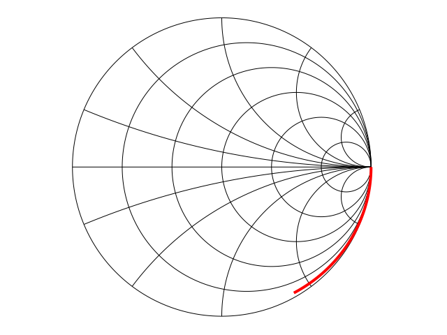
define(S12(s),block([Z_0],Z_0:50,ev(S[1,2])))$
S12(s);
/* S12 is a TRANSMISSION coefficient; a Smith chart maps REFLECTION
   coefficient.  Plot its magnitude against frequency instead. */
wxplot2d(20*log10(cabs(S12(%i*2*%pi*f*1e9))),
    [f,0.001,100],
    [logx],
    [legend,false],
    [xlabel,"Frequency [GHz]"],
    [ylabel,"dB20(|S12|) [dB]"],
    [style,[lines,3,2]],
    [gnuplot_preamble,"set grid"]);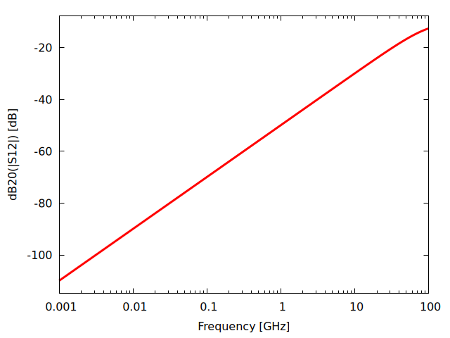
define(S21(s),block([Z_0],Z_0:50,ev(S[2,1])))$
S21(s);
/* S21 is a TRANSMISSION coefficient; a Smith chart maps REFLECTION
   coefficient.  Plot its magnitude against frequency instead. */
wxplot2d(20*log10(cabs(S21(%i*2*%pi*f*1e9))),
    [f,0.001,100],
    [logx],
    [legend,false],
    [xlabel,"Frequency [GHz]"],
    [ylabel,"dB20(|S21|) [dB]"],
    [style,[lines,3,2]],
    [gnuplot_preamble,"set grid"]);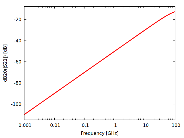
define(S22(s),block([Z_0],Z_0:50,ev(S[2,2])))$
S22(s);
PlotSmithChart([
    parametric,
    realpart(S22(%i*%omega)),
    imagpart(S22(%i*%omega)),
    [%omega,2*%pi*1e6,2*%pi*100e9],
    [nticks,1000]]);